Electronics / Integrated Circuits
User Manual for ALFA 1100SK2, K1100SK2, KP1100SK2 Analog Signal Sample-and-Hold ICs
Technical guide for ALFA 1100SK2, K1100SK2, and KP1100SK2 sample-and-hold integrated circuits. Includes pinout configurations, electrical parameters, maximum ratings, and functional diagrams.
Table of contents
Manual images
Click an image to enlargeQuick guide from the manual
The ALFA 1100SK2, K1100SK2, and KP1100SK2 are integrated circuits designed for analog signal sampling and holding. Upon receiving a command at the control input, the device captures the instantaneous value of the input signal and maintains a constant output voltage with high precision. Users must ensure the power supply matches the specific version (±12V for version A, ±15V for version B) and that input signals remain within the specified ±5V range to prevent permanent damage.
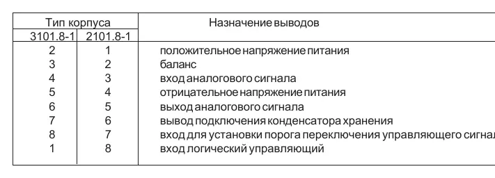
Pinout and Connections
The manual provides pinout assignments for two package types: 3101.8-1 and 2101.8-1. Users must verify the package type before connecting the device to ensure correct signal routing, including power supply pins, analog input, output, and control inputs.
Electrical Parameters
The device operates within a temperature range of 0 to 70°C. Key performance metrics include:
- Sampling Time: Typically 7µs (at 0.1% accuracy with 1000pF capacitor).
- Aperture Delay: Maximum 180ns.
- Input Voltage Range: ±5V.
- Control Compatibility: Compatible with TTL/CMOS logic levels.
Maximum Ratings
Exceeding the specified maximum ratings can cause irreversible damage to the integrated circuits. Users must strictly adhere to the limits defined for supply voltage (positive and negative polarity) and input voltage. The manual provides specific tables for the 'Maximum Permissible Mode' and 'Limit Mode' to guide safe operation.
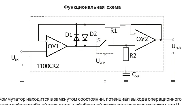
Functional Diagram
The functional schematic illustrates the internal architecture, including the operational amplifiers (OY1, OY2), switches, and the connection points for the external storage capacitor (CXP). This diagram is essential for understanding the signal path and the role of external components in the sampling process.
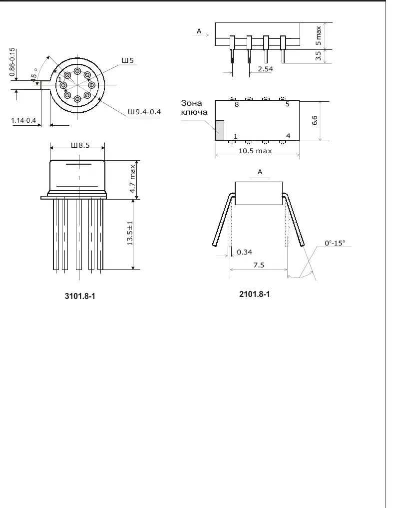
Dimensional Drawings
Detailed mechanical drawings are provided for both package types (3101.8-1 and 2101.8-1), including all necessary dimensions for PCB layout and mounting.
Manufacturer information
Joint Stock Company ALFA
Practical help
Common problems
Permanent damage to the IC
Ensure that supply voltages and input voltages do not exceed the values listed in the 'Limit Mode' (Предельный режим) table.
Incorrect output signal
Verify that the external storage capacitor (CXP) is correctly connected and that the control input signal is within the required logic levels.
Before use
- Identify the specific IC version (A or B) to determine the correct supply voltage (±12V or ±15V).
- Confirm the package type (3101.8-1 or 2101.8-1) to ensure correct pinout mapping.
- Ensure the input signal range is within ±5V.
- Verify that the control input is compatible with TTL/CMOS logic levels.
- Check that the power supply is stable and within the specified limits.
Specs in practice
- Supply Voltage (UП)
- The operating voltage required for the IC. Version A requires ±12V, while Version B requires ±15V.
- Aperture Delay
- The time delay between the control command and the actual sampling of the signal; must be less than 180ns.
- Sampling Time
- The time required to sample the signal with 0.1% accuracy, typically 7µs.
Images and diagrams
- The pinout table maps physical pins to functions like positive/negative power, analog input/output, and control inputs.
- The functional schematic shows the internal Op-Amps and the connection point for the external storage capacitor (CXP).
Model compatibility
- The control input is compatible with standard TTL and CMOS logic levels.

Manual page author
Michael Turner
Technical manual editor
Reviews PDF manuals for structure, safety notes, and practical product details so readers can find the right information quickly.