Power / Uninterruptible Power Supplies
Reference Manual for Toshiba 12-bit Analog to Digital Converter (ADC-G)
Comprehensive reference manual for the Toshiba 12-bit Analog to Digital Converter (ADC-G). Includes configuration, operation modes, register details, and usage examples for general purpose and PMD trigger conversions.
Table of contents
Manual images
Click an image to enlargeQuick guide from the manual
This document provides technical specifications and operational instructions for the Toshiba 12-bit Analog to Digital Converter (ADC-G). It covers the configuration of the ADC, including clock supply, start-up factors, and monitor functions. Users should refer to this manual for register settings, conversion timing calculations, and integration with peripheral functions like the Programmable Motor Control Circuit (PMD).
ADC Configuration and Signals
The ADC unit converts multiple analog inputs (AINx00 to AINx24) to digital values. Key components include:
- Conversion Control: Manages start-up factors and conversion programs.
- PMD Trigger Control: Synchronizes ADC conversion with motor drive timing.
- General Purpose Start-up: Supports software-triggered single or continuous conversions.
- AD Monitor Function: Allows monitoring of conversion results against set values to trigger interrupts or protection signals.
Operation Modes
The ADC supports several conversion modes:
- General Purpose Start-up: Triggered by software or general purpose timer inputs. Supports single and continuous conversion modes.
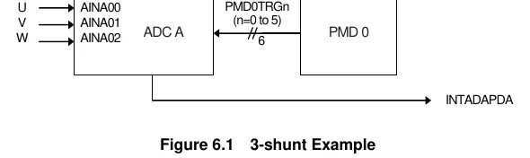
- PMD Trigger Conversion: Triggered by PMD signals, allowing synchronized conversion for motor control applications (e.g., 3-shunt or 1-shunt configurations).
Conversion Timing and Settings
Conversion time is calculated as the sum of sampling time and comparison time. Users must configure the following based on power supply voltage (AVDD5) and SCLK frequency:
- Sampling Time: Configurable via [ADxCLK] and [ADxMOD1] registers.
- Conversion Time: Varies depending on the SCLK frequency (20MHz or 30MHz) and voltage range (2.7V to 5.5V).
AD Monitor Function
The monitor function compares conversion results against a reference value. It supports:
- Determination Conditions: Larger or smaller than the comparison register.
- Count Conditions: Continuous count or accumulated count to trigger an interrupt (INTADxCP0/1).
Register Overview
The ADC is controlled via memory-mapped registers. Key registers include:
- [ADxCR0] / [ADxCR1]: Control registers for enabling ADC, starting conversions, and configuring DMA requests.
- [ADxST]: Status register to check conversion progress.
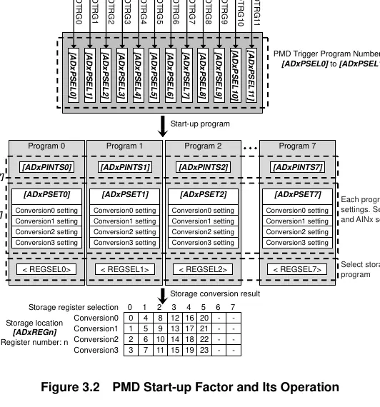
- [ADxTSETn]: General purpose start-up factor program registers.
- [ADxPSETn]: PMD trigger program registers.
- [ADxREGn]: Conversion result storage registers.
Usage Examples
The manual provides specific sequences for:
- Single Conversion: Setting up interrupts, configuring DAC, and initiating conversion via software.
- PMD Trigger Conversion: Configuring trigger assignments and program registers for synchronized motor control (3-shunt and 1-shunt examples).
Precautions
To ensure accuracy, avoid changing output pin data during conversion. Use bypass capacitors between AVDD5/AVSS and VREFHx/VREFLx pins to minimize digital noise.
Practical help
Common problems
AD conversion accuracy degradation
Ensure output pins do not change during conversion; use the mean value of multiple conversion results if necessary.
Digital noise interference
Insert a bypass capacitor between AVDD5 and AVSS pins, and between VREFHx and VREFLx pins, placed as close to the terminal as possible.
Before use
- Verify power supply voltage (AVDD5) is within the specified range (2.7V to 5.5V).
- Ensure the ADC conversion clock is enabled in the relevant register.
- Check that AD conversion has stopped before changing operation modes or stopping the clock.
- Set [ADxMOD0] to '1' and wait at least 3µs for stabilization before starting conversion.
Specs in practice
- Conversion resolution
- 12 bits.
- Conversion time
- Calculated as Sampling time + Comparison time; varies by voltage and SCLK frequency.
Images and diagrams
- Figure 1.1: Connection relationships between ADC and peripheral functions like PMD and timers.
- Figure 2.1: ADC Block Diagram showing registers, control logic, and signal paths.
- Figure 3.6: Conversion timing diagram showing sampling and comparison phases.
- Figure 4.1: Equivalent circuit of the analog input pin.
Model compatibility
- Compatible with Advanced Programmable Motor Control Circuit (PMD) and Programmable Motor Control Circuit Plus.

Manual page author
David Miller
Documentation analyst
Organizes user manual content into clear summaries, with attention to model details, product context, and everyday usability.