Electronics / Monitors
EVAL-LT8418-AZ 100V Half-Bridge GaN Driver Evaluation Board
User guide for the EVAL-LT8418-AZ evaluation board, featuring the LT8418 100V half-bridge GaN driver with smart integrated bootstrap switch, optimized for high-efficiency power conversion.
Table of contents
Product Overview
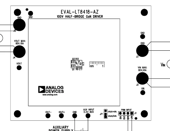
The EVAL-LT8418-AZ is an evaluation circuit designed to demonstrate the performance of the LT8418, a 100V half-bridge driver for enhanced Gallium Nitride (eGaN) FETs. The board is primarily optimized for buck converter applications but is versatile enough to support boost and other half-bridge topologies. It is capable of delivering up to 10A of output current with effective thermal management.
Key Features and Performance
The LT8418 driver integrates a smart bootstrap switch to ensure balanced bootstrap voltage with minimal dropout. It features powerful 0.2Ω pull-down and 0.6Ω pull-up drivers. The board includes split gate drivers, allowing users to adjust turn-on and turn-off slew rates to suppress ringing and optimize EMI performance. Under typical conditions (48V input, 24V output, 1MHz), the board achieves high efficiency, exceeding 97%.
Setup and Operation
The board operates in an open-loop configuration and requires external PWM signals. The default setup uses a single-PWM-input mode, where onboard dead-time circuitry generates the necessary complementary signals. For advanced users, a dual-PWM-input mode is available by modifying specific resistors (R5, R7, R3, R6) to bypass the RC filters. Users must be careful in dual-input mode to prevent shoot-through conditions.
Thermal Considerations
Due to the high switching frequencies and power levels, thermal management is critical. The board includes four mechanical spacers to facilitate the attachment of a heat sink (527-45AB) to the top layer. A thermal pad should be used between the heat sink and the GaN FETs/LT8418 to ensure optimal heat dissipation. Forced airflow is recommended for extended operation at full load.
Measurement and Probing
For accurate measurement of high-frequency waveforms, particularly the high-side gate voltage, a high-speed differential probe (e.g., Tektronix IsoVu) is recommended. When probing gate signals or the switch node, use a ground spring to minimize parasitic inductance. Voltage ripple measurements should be taken directly across the input or output terminals using low-capacitance passive probes.
Manufacturer information
Analog Devices, Inc.
Practical help
Common problems
Overheating of GaN FETs
Ensure a heat sink is attached using the provided spacers and thermal pad; consider forced airflow for high-load, extended operation.
Shoot-through in dual-PWM mode
Ensure precise control of the two independent PWM signals, as the onboard dead-time circuitry is bypassed in this configuration.
High ringing on switch node
Adjust the turn-on and turn-off slew rates using the split gate driver configuration or verify probe connection using a ground spring.
Before use
- Ensure all power supplies are turned off before making connections.
- Connect input power supply to VIN and GND terminals.
- Connect auxiliary power supply to AUX INPUT and GND terminals.
- Connect load to VOUT and GND terminals.
- Connect function generator to INT and GND pins of header J1.
- Set auxiliary power supply to 6V.
- Verify all jumper and resistor configurations match the desired control mode.
Images and diagrams
- Figure 1 illustrates the standard connection setup for the board in single-PWM-input control mode.
- Figure 2 shows the relationship between resistor values (R3, R6) and the resulting dead times.
- Figure 17 provides the full electrical schematic for the evaluation board.
Model compatibility
- The board is designed for 100V eGaN FETs.
- Requires external PWM signals from a function generator or microcontroller.
- Compatible with various converter topologies including buck and boost.

Manual page author
David Miller
Documentation analyst
Organizes user manual content into clear summaries, with attention to model details, product context, and everyday usability.