Power / Batteries Chargers
User Guide for Diodes Incorporated 18W QC3.0 SSR Premium Charger EV1 Board
Quick start guide and technical documentation for the Diodes Incorporated 18W QC3.0 SSR Premium Charger EV1 evaluation board, including connection procedures, specifications, and testing results.
Table of contents
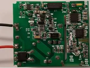
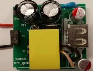
Manual images
Jump to the sectionQuick guide from the manual
This document serves as a technical user guide for the 18W QC3.0 SSR Premium Charger EV1 evaluation board. It provides essential information for engineers and developers to set up, connect, and test the charger board. The board is designed for high-efficiency, cost-effective QC3.0 charging applications.
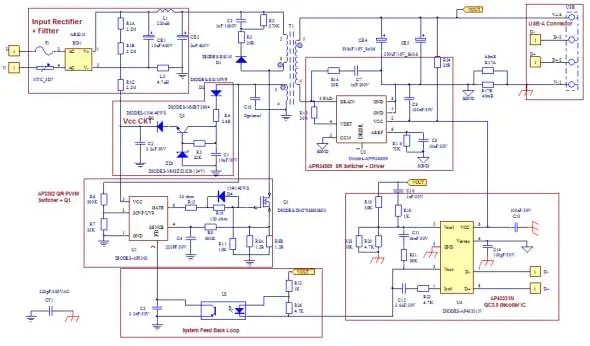
System Overview
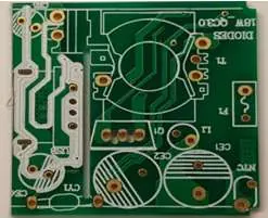
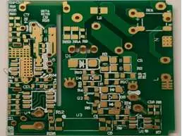
The EV1 board is composed of three primary components: the AP3302 PWM controller, the APR34509 synchronous rectification switcher, and the AP43331N QC3.0 decoder. It supports a wide input voltage range (90Vac to 264Vac) and provides constant voltage (CV) and constant current (CC) modes.
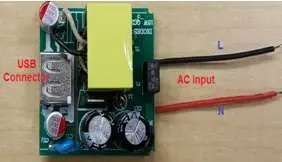
System Setup and Connections
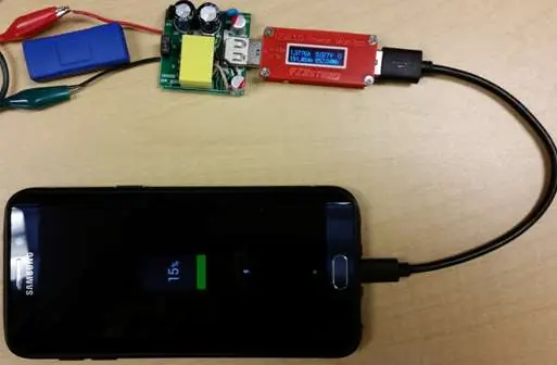
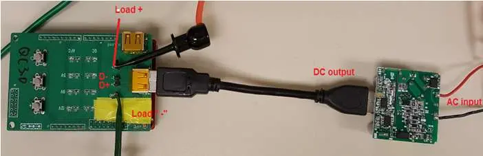
Before connecting the board, ensure the AC source is switched off. The setup requires a Diodes 18W QC3.0 & 2.0 Test Kit, a USB 3.0 to Micro B cable, and an electronic load (or a QC3.0-equipped smartphone). Connect the AC input L and N wires to the power supply output. Use banana jack cables to connect the E-load to the board's output terminals.
Testing Procedures
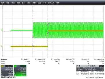
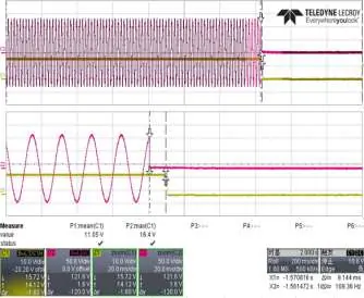
The charger defaults to 5V upon startup. Use the buttons on the test kit to cycle between QC2.0 and QC3.0 modes. In QC3.0 mode, the output voltage can be adjusted in 200mV increments between 3.6V and 12V using the '+' and '-' buttons.
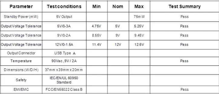
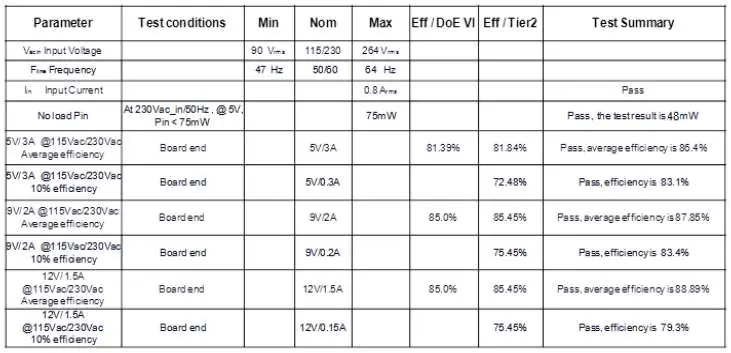
Technical Specifications
- Input Voltage: 90Vac to 264Vac
- Output Power: <= 18W
- Efficiency: 87.5%
- Standby Power: < 75mW
- Dimensions: 37 x 39 x 20 mm
- Protections: OVP, UVP, OLP, BNO, FOCP, SSCP, OTP
Safety and Compliance
The board meets DOE6 and CoC Tier 2 efficiency requirements and is RoHS compliant. It is designed for evaluation purposes and should be handled with appropriate safety precautions for high-voltage AC circuits.
Manufacturer information
Diodes Incorporated
Practical help
Common problems
Charger not outputting expected voltage
Ensure the test kit is in the correct mode (QC2.0 or QC3.0) and verify the connection to the E-load.
High standby power
Verify that no load is connected and that the input voltage is within the specified 90-264Vac range.
Before use
- Ensure AC power source is switched OFF before making connections.
- Prepare a Diodes 18W QC3.0 & 2.0 Test Kit.
- Prepare a one-foot USB 3.0 to Micro B cable.
- Verify that the E-load is ready for connection to the output terminals.
- Check that all wiring (AC L & N) is secure.
Specs in practice
- Input Voltage
- The board operates between 90Vac and 264Vac.
- Output Power
- Maximum total constant output power is 18W.
- Standby Power
- No-load power consumption is less than 75mW.
Images and diagrams
- Figure 3: Full schematic of the EV1 board showing input filtering, PWM controller, and feedback loop.
- Figure 10: Visual guide for connecting the test kit and E-load to the board.
- Figure 11: Identification of the voltage adjustment buttons on the test kit.
Model compatibility
- Supports Qualcomm QC 3.0 and QC 2.0 protocols.
- Designed for use with USB Type A output connectors.
- Not authorized for use as a critical component in life support systems.

Manual page author
Michael Turner
Technical manual editor
Reviews PDF manuals for structure, safety notes, and practical product details so readers can find the right information quickly.