Electronics / Evaluation Boards
Quick Start Guide for Linear Technology Demonstration Circuit 1019A
Quick start guide for the Linear Technology 1019A Dual White LED Driver Converter. Includes setup procedures, jumper configurations, performance specifications, and measurement instructions.
Table of contents
Manual images
Click an image to enlargeQuick guide from the manual
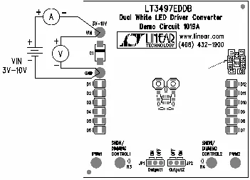
The Demonstration Circuit 1019A is a Dual White LED Driver Converter featuring the LT3497. It is designed to drive two independent LED strings at 20mA from a 3V-10V input. Before operating, ensure the input voltage does not exceed 10V. The board includes jumpers (JP1, JP2) that must be configured for testing.
Description
The 1019A demo circuit demonstrates the small size and low component count of the LT3497 in a 3mm x 2mm DFN package. It features internal Schottky diodes, high switching frequency, and internal open circuit protection. The board allows for various dimming controls, including optional N-MOSFET placeholders for direct PWM dimming.
Performance specifications
The following performance parameters are measured at TA = 25°C:
- Input Supply Range (VIN): 3V to 10V
- Output Current (IOUT): 20mA (19mA min, 21mA max)
- Output Voltage (VOUT): 19.5V
- Efficiency: 72.3% (at VIN=3.6V)
- Switching Frequency (Fs): 2.3 MHz (1.8 MHz min, 2.8 MHz max)
- Quiescent Current (IQ): 15mA (at VIN=4.2V, CTRL=ON, LEDs open)
- Quiescent Current in Shutdown (IQSHDN): 10µA (at VIN=4.2V, CTRL=OFF)
Quick start procedure
- Place jumpers JP1 and JP2 in the ON position to test the circuit.
- With the power off, connect the input power supply to the VIN and GND terminals.
- Turn on the power at the input. Ensure the input voltage does not exceed 10V.
- Check for proper voltages and currents. If LEDs do not light up, verify jumper settings.
- Once operations are established, adjust the input within the operating range to observe parameters.
Measurement setup
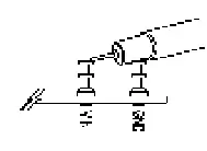
When measuring input or output voltage ripple, avoid using a long ground lead on the oscilloscope probe. Measure the ripple by touching the probe tip directly across the VIN or VOUT and GND terminals.
Dimming control
To test filtered PWM dimming or direct DC dimming, remove jumper JP1 or JP2. Apply the PWM or DC signal to the SHDN/DIMMING CTRL1 or SHDN/DIMMING CTRL2 terminals and observe the LED output brightness. For direct PWM dimming, refer to the specific section in the LT3497 datasheet.
Safety warnings
WARNING: Do not look directly at the operating LED. This circuit produces light that can damage eyes.
Schematic
The demonstration circuit includes design files and a schematic layout for the LT3497EDDB, which can be referenced for modifying the circuit or understanding the component connections.
Practical help
Common problems
LEDs do not light up
Check the jumper settings (JP1 and JP2) to ensure they are in the correct position.
Input voltage ripple measurement is inaccurate
Avoid using a long ground lead on the oscilloscope probe. Touch the probe tip directly across the VIN or VOUT and GND terminals.
Input voltage exceeds limits
Ensure the input voltage does not exceed 10V, as the circuit is limited by the maximum input voltage of the LT3497.
Before use
- Ensure the input power supply is turned off before connecting.
- Verify that the input power supply is connected to VIN and GND.
- Set jumpers JP1 and JP2 to the ON position.
- Ensure the input voltage is within the 3V-10V range.
Images and diagrams
- Figure 1 illustrates the proper measurement equipment setup, showing the connection of the power supply and the placement of jumpers.
- Figure 2 demonstrates the correct oscilloscope probe technique for measuring voltage ripple.
Model compatibility
- The demo circuit is specifically designed for the LT3497EDDB.
- Input voltage must be kept between 3V and 10V.

Manual page author
Michael Turner
Technical manual editor
Reviews PDF manuals for structure, safety notes, and practical product details so readers can find the right information quickly.