Electronics / Evaluation Boards
User Guide for Linear Technology Demonstration Circuit 1255
Quick start guide for the Linear Technology Demonstration Circuit 1255 (16-bit, 250ksps ADC). Includes setup instructions, power requirements, jumper configurations, and data collection procedures.
Table of contents
Manual images
Click an image to enlargeQuick Guide from the Manual
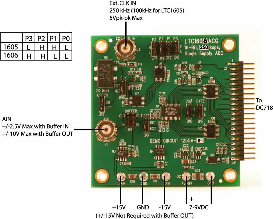
The Demonstration Circuit 1255 (DC1255) is an evaluation board designed for the LTC1605 and LTC1606 16-bit ADCs. This guide provides the necessary steps to connect, power, and configure the board for performance evaluation using the Pscope software.
Quick Start Procedure
- Connect the DC1255A board to a DC718B USB High Speed Data Collection Board using connector J2.
- Connect the DC718B to a host PC using a standard USB A/B cable.
- Apply 7-9VDC to the 7V-9V and GND terminals.
- If using the internal buffer (default), apply +15V and -15V to the indicated terminals.
- Connect your signal source to connector J1.
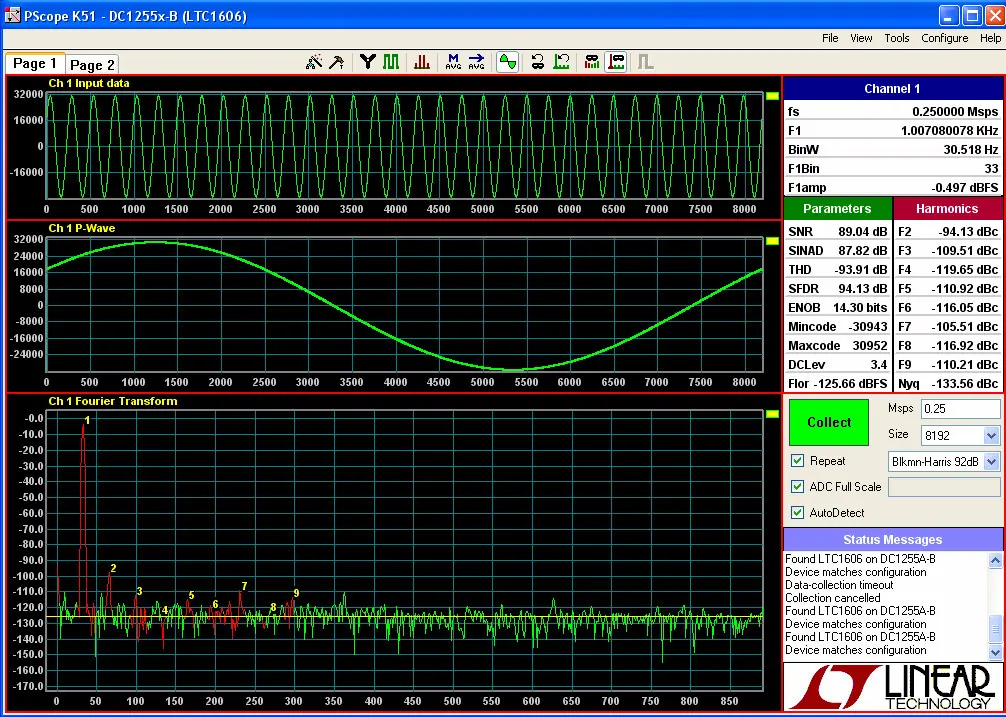
- Run the QuickEval-II software (Pscope.exe version K51 or later) on your PC.
- Click the Collect button in the software to begin data acquisition.
DC1255 Setup
DC Power
The board requires 7-9VDC at approximately 24mA. The +/-15V supply is required only if you are using the input amplifier (U3). If you bypass the amplifier using jumper JP1, the +/-15V supply is not needed.
Clock Source
The board can be clocked internally or externally:
- Internal Clock: Default setting. Uses an ECS 1MHz clock oscillator. JP9 (OSCEN) can turn the oscillator off. Jumpers JP4-JP7 set the internal clock divider ratio.
- External Clock: Provide a low jitter 10dBm sine or square wave to connector J3. Note that J3 has a 50-ohm termination resistor to ground.
Analog Input
The board is shipped with JP1 in the IN position, placing the input amplifier (LT1468) in the signal path, which provides a gain of 9dB. Setting JP1 to the OUT position removes the amplifier, resulting in an input impedance of 10k-ohm at J1.
Jumpers and Reference
- BYTE (JP3) and CS# (JP8): Typically tied to ground. Jumpers allow for external signal introduction.
- Reference (JP2): Allows selection between the on-chip reference or an external LT1019A-2.5 reference (default).
Data Collection
For optimal performance, ensure the system used for data collection does not produce significant ground current through the demo board. The board does not include an anti-aliasing filter; if required, it should be placed prior to the LT1468 or any external amplifier in the signal path.
Official resources from the manual
Practical help
Common problems
Software does not acquire data
Ensure the DC718B is connected and recognized by Pscope. Press the 'Collect' button; if the board was previously used, you may need to press it a second time.
High noise or distortion
Check for ground potential differences between instruments. If using high gain, consider transformer isolation.
Clock signal issues
If using an external clock, ensure it is a low jitter 10dBm sine or square wave. Driving J3 with logic signals may be difficult due to the 50-ohm termination.
Before use
- Connect DC1255A to DC718B via connector J2.
- Apply 7-9VDC power to the 7V-9V and GND terminals.
- Apply +/-15V if using the internal amplifier (U3).
- Connect signal source to J1.
- Install and run Pscope.exe (QuickEval-II software).
Images and diagrams
- Figure 1 shows the connection diagram, including power terminals, signal input (J1), and jumper locations.
- Figure 2 displays the Pscope software interface for data collection.
Model compatibility
- Designed for LTC1605 and LTC1606 ADCs.
- Requires DC718B USB High Speed Data Collection Board for PC interface.

Manual page author
Emily Carter
User documentation editor
Prepares concise manual descriptions and highlights the most useful setup, operation, and maintenance information for readers.