Industrial / I/O Modules
User Manual for ACCES I/O 104-DIO-24E Digital I/O Board
Comprehensive user manual for the ACCES I/O 104-DIO-24E digital I/O board. This guide provides essential information on hardware installation, jumper configuration for base addresses and IRQs, programming examples, and detailed connector...
Table of contents
Manual images
Click an image to enlargeQuick Guide
The 104-DIO-24E is an industrial digital I/O board designed for PC/104 bus systems. It features 48 bits of digital I/O, software-controlled interrupt generation, and optional 8254 counter/timer functionality. The board is compatible with industry-standard I/O racks such as Opto-22, Gordos, and Potter & Brumfield.
Hardware Installation
Before installing the board, ensure the computer power is completely off. Connecting or disconnecting cables while the system is powered can damage the board and void the warranty.
- Configure jumpers for selected options and base address according to your application requirements.
- Remove power from the PC/104 stack.
- Assemble standoff hardware for stacking and securing the boards.
- Carefully plug the board onto the PC/104 connector on the CPU or onto the stack, ensuring proper alignment of the pins.
- Install I/O cables onto the board’s I/O connectors.
- Check all connections in the PC/104 stack before powering up the system.
- Run the provided sample programs from the CD to validate the installation.
Option Selection
The board uses jumpers to configure key settings:
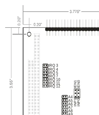
- IRQ Level: Seven jumpers are used to select the IRQ level (IRQ2-IRQ7, IRQ10-IRQ12).
- Base Address: Six jumpers (A4-A9) select the base address within the 000-3F0 hex range.
- Interrupts: External interrupts are accepted on pin 9 (bit C3). Jumpers must be installed in the IEN or INP position for interrupts to function.
- I/O Buffers: The 74LS245 buffers can be enabled/disabled via the TST/BEN jumper.
Programming
The board is an I/O-mapped device. The recommended programming languages for interrupt service routines are Delphi or C++ Builder. Visual BASIC is not recommended for interrupt-type programming.
I/O Mapping: The board occupies 16 bytes of I/O space. The counter/timer shares the same I/O space as Digital I/O Group 0. To 'map in' the counter/timer, write any value to Base Address + Dh. To 'map out' and re-enable access to the DIO, read from Base Address + Dh.
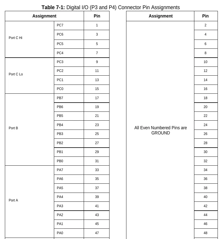
Connector Pin Assignments
The board uses two 50-pin headers (P3 for Group 0, P4 for Group 1). Every second pin is grounded to minimize crosstalk. Refer to the connector pin assignment tables in the manual for specific signal locations (PA0-PA7, PB0-PB7, PC0-PC7).
Safety and Warnings
Warning: Always connect and disconnect field cabling with the computer power off. Installing boards into a system with power on may cause permanent damage to the I/O board and will void all warranties.
Practical help
Common problems
Unpredictable computer behavior
Check for address overlap. Ensure the base address jumpers are set correctly and do not conflict with other installed functions.
Interrupts not functioning
Ensure a jumper is installed in either the IEN or INP position. Verify that the interrupt is cleared by writing to base address + Fh.
I/O buffers not working
Check the TST/BEN jumper position. If in TST mode, the buffer state is controlled by a register.
Before use
- Power off the PC/104 stack completely before installation.
- Configure base address and IRQ jumpers based on your system requirements.
- Install the provided software from the CD.
- Verify that the PC/104 stack has the necessary clearance for the board.
- Ensure all I/O cables are securely connected to the 50-pin headers.
Specs in practice
- Digital Inputs
- TTL compatible; Logic High: 2.0 to 5.0 VDC; Logic Low: -0.5 to +0.8 VDC.
- Digital Outputs
- Source 32mA, Sink 64mA; Logic High: 2.5 VDC min; Logic Low: 0.5 VDC max.
- Operating Temperature
- 0°C to +70°C (Standard); -40°C to +85°C (Optional).
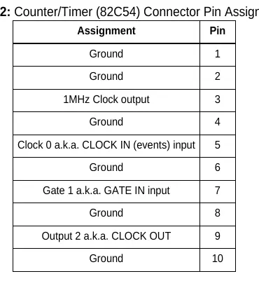
- Counter/Timer
- 82C54 programmable interval counters; 16-bit event counter or 32-bit rate generator.
Images and diagrams
- Figure 1-1: Block diagram showing the relationship between the PC/104 bus, PPI groups, and counter/timer.
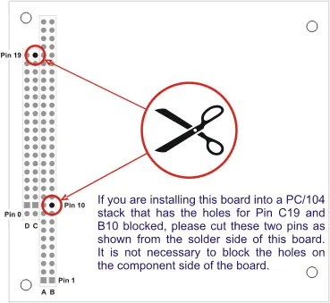
- Figure 2-1: PC/104 key information regarding pin cutting for specific stack configurations.
- Figure 3-1: Option selection map showing jumper locations for IRQ and address configuration.
Model compatibility
- Compatible with industry standard I/O racks like Opto-22, Gordos, and Potter & Brumfield.
- Designed for 16-bit or 8-bit PC/104 bus sockets.

Manual page author
David Miller
Documentation analyst
Organizes user manual content into clear summaries, with attention to model details, product context, and everyday usability.